- On sale!
Reference: DWM14042301
Spring antenna is specialized for wireless data transmission. This antenna with good performance of V.S.W.R, small size design, easily installation, stable performance and good anti-shock and anti-aged compatible for Hoperf Modules.
Reference: DWM14032902
SMA rf antenna connector is pallets copper gold andexternal thread needle sma pallets plate rf connector.
Reference: DWM14032102
Whip antenna for sub-1 GHz, 433MHz,868MHz and 915MHz with SMA male connectors.it's used with wireless module recommanded by Hoperf .
Reference: DWM14042401
SMA RG178 extension female cable for GPS, GSM antenna,RF module, SMA cable,IPEX to SMA jumper cable.
Reference: DWM18032302
USD3.0/pcs MOQ100pcs LoRa Antenna designed for Lora application which required for outdoor waterproof highgain and work at ISM free band like 433MHz /868MHz /915MHz SMA Male Whip antenna.
Reference: DWM16121503
DWM-TLB-3.0QB SUB-1GHz / 2.4GHz Whip antenna with a Collapsible SMA male connectors.Which are available for 433MHz,868MHz.915MHz and 2.4GHz..
Reference: DWM17111002
LoRa Antenna-433MHz High Gain internal aerial piamater FPC Antenna with IPEX connctor.
Reference: DWM15101001
Brand: Semtech
RFM50 module series’ design is based on the high performance RF50 SoC chip, It include a CIP-51 core‘ MCU and 100mW transceiver. It operate at 433/470/868/915 MHz ISM band, comply with FCC, ETSI regulation.

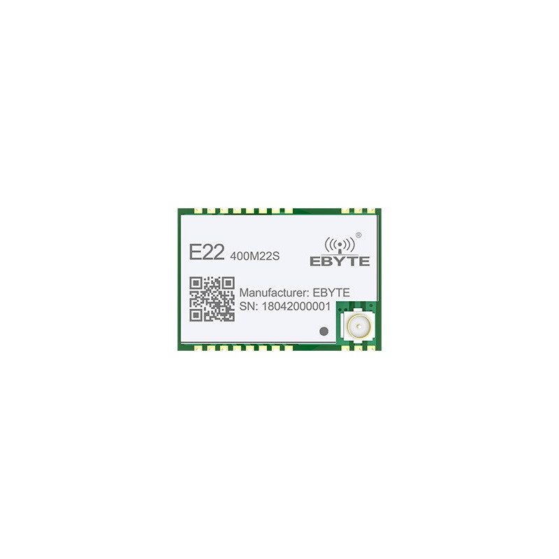
The E22-M22S 433MHz /868MHz /915MHz SPI +30dBm Enhanced Power LoRa Transceiver Module is based on original imported RFIC SX1268(433MHz) and SX1262(868MHz/915MHz) from SEMTECH, adopts LoRa spread spectrum technology.
The E22-M22S series is the first wireless module in China to adopt Semtech's SX1268, SX1262 RF chip. This chip provides a variety of modulation methods, such as LoRaTM and traditional GFSK. Its special LoRaTM modulation method increases the communication distance.
| RF Parameter | Value |
Remark |
| Working frequency |
410~493 MHz,850~930 MHz | |
| Transmitting power | 22 dBm |
Max. Power (160mW) |
| Receiving sensitivity | -147 dBm |
- |
| Air data rate | 0.018k~300kbps |
- |
| Test distance | 6500m |
In open and clear air, with maximum power, 5dBi antenna gain, height of 2m |
| Hardware Parameter | Value |
Remark |
|
Size |
14 * 20 mm |
|
|
Antenna type |
IPEX / Stamp hole |
|
|
Communication interface |
SPI |
|
|
Package |
SMD |
|
| Electronic parameter | Min. | Typ. | Max. | Unit | Condition |
| Power supply |
1.8 | 3.3 | 3.6 | V | |
| Communication level | 1.8 | 3.3 | 3.6 | V | |
| Transmitting current |
95 | 100 | 105 | mA | 22dBm(160mW) |
| Receiving current |
6 |
6.5 | 7 | mA | |
| Sleep current |
1 |
2 | 3 | nA | |
| Operating temperature |
-40 | 20 |
+85 | ℃ | |
| Operating humidity |
10 | 60 |
90 | % | |
| Storage temperature |
-40 | 20 |
+125 | ℃ |
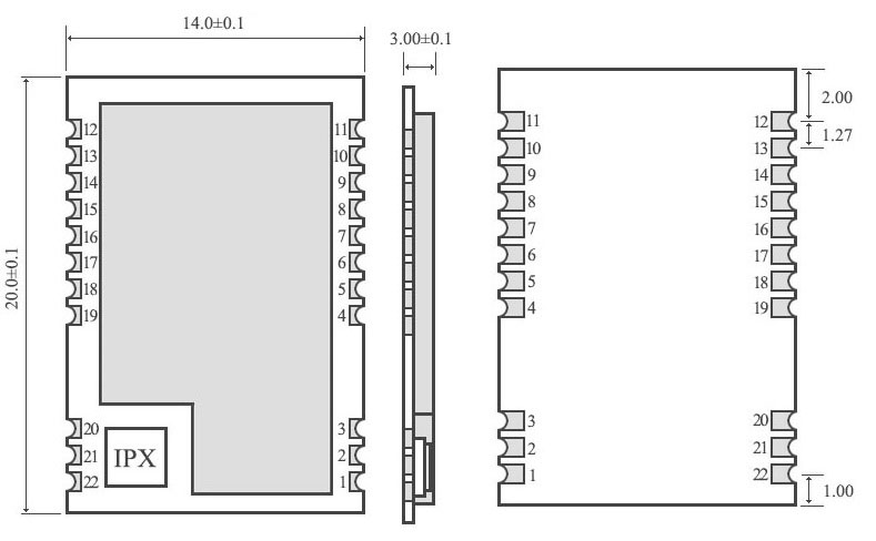
| Pin No. |
Pin Item | Pin Direction | Pin Application |
|
1 |
GND |
- |
Ground |
|
2 |
GND |
- |
Ground |
|
3 |
GND |
- |
Ground |
|
4 |
GND |
- |
Ground |
|
5 |
GND |
- |
Ground |
|
6 |
RXEN |
Input |
RF switch RX control,connecting external MCU IO, valid in high level |
|
7 |
TXEN |
Input |
RF switch TX control,connecting external MCU IO or DIO2, valid in high level |
|
8 |
DIO2 |
Input/Output |
Configurable IO port(see more SX1262,Sx1268 datasheet) |
|
9 |
VCC |
- |
Power supply, 2.5V~5.5V(external ceramic filter capacitoris recommended) |
|
10 |
GND |
- |
Ground |
|
11 |
GND |
- |
Ground |
|
12 |
GND |
- |
Ground |
|
13 |
DIO1 |
Input/Output |
Configurable IO port(see more in SX1262,Sx1268 datasheet) |
|
14 |
BUSY |
Output |
State indicator(see more in SX1262,Sx1268 datasheet) |
|
15 |
NRST |
Input |
Chip reset initiation, valid in low level |
|
16 |
MISO |
Output |
SPI master input slave output |
|
17 |
MOSI |
Input |
SPI master output slave input |
|
18 |
SCK |
Input |
SPI clock |
|
19 |
NSS |
Input |
Chip select,for starting a SPI communication |
|
20 |
GND |
- |
Ground |
|
21 |
ANT |
- |
Stamp hole(50 ohm impedance) |
|
22 |
GND |
- |
Ground |
n No
Reference: DWM14073001
Brand: Semtech
APC340 LoRa series rf module is built in RFIC sx1278 and sx1276 which can work on 433MHz,470MHz ,868MHz,915MHz 20dBm Ultra Long Range Transceiver Module with LoRa spread spectrum modulation.
Reference: DWM15123001
Brand: Semtech
HM-TRLR-S series are operating at 433MHz, 868MHz, 915MHz low cost, high performance transparent transceiver with LoRa/FSK/ GFSK/OOK modulation variety.It's mainly use for uav controller and drone data link.
Reference: DWM16092701
RFM98PW/ RFM95PW which are Enhanced Power Long Range Transceiver Module.the available versions is RFM98PW 433MHz, and 868MHz,915MHz for RFM95PW.
Reference: DWM16112801
DWM-LoRa1276F30 is a 500W high power wireless transceiver module, which integrates SemtechRF transceiver chip SX1276. There are 868MHz and 915MHz for avaialble options.
Reference: DWM16112802
DWM-LoRa1278F30 is a 500W high power wireless transceiver module, which integrates SemtechRF transceiver chip SX1278. There are 433MHz and 470MHz for avaialble options.
Reference: DWM20021902
Brand: Semtech
Free Shipping DWM-LJ1276 868MHz /915MHz sx1276 LoRa transceiver RF module which core chipset are the semtech SX1276 LoRa chipset,usually build for the ARM application.
Reference: DWM18021804
M5Stack NEO-M8N GPS Module for ESP32 Development Kit with Internal & External Antenna MCX Interface.
Reference: DWM18103005
USD74/pcs MOQ100 The OLG01 is an Water proof outdoor setting open source single channel LoRa Gateway. It lets you bridge LoRa wireless network to an IP network via WiFi, Ethernet, 3G or 4G cellular.
Reference: DWM16011801
Brand: Semtech
LoRa1276 Wireless Transceiver Module adopts Semtech RF transceiver chip SX1276 which LOS transmission distance can reach to 4km~6km Long Distance.
Reference: DWM14033102
Brand: Semtech
The RFM96W / RFM98W 433MHz,470MHz transceivers feature the LoRaTM long range modem It's from the HopeRF LoRa module.build by the semtech chipset with the application for ARM meters.
Reference: DWM14073001
Brand: Semtech
APC340 LoRa series rf module is built in RFIC sx1278 and sx1276 which can work on 433MHz,470MHz ,868MHz,915MHz 20dBm Ultra Long Range Transceiver Module with LoRa spread spectrum modulation.
Reference: DWM20060102
Brand: Semtech
DWM-RAK4200 Breakout Module is specifically designed to allow easy excess to the pins on the module in order to simplify development and testing.it's utilized is of an Xbee form factor.
Reference: DWM18011801
DWM-RAK83 433MHz/ 868MHz/ 915MHz SX1301 LoRa/ LoRaWAN Gateway Module combine a host system like Raspberry Pi or WisAP(OpenWRT based) or WisCam to help you realize the whole Lora system development.
Reference: DWM20053103
Brand: Semtech
The DWM-RAK4600 development board allows access to all serial and GPIO ports for easy configuration. The RAK4600 core module includes nRF52832 MCU and SX1276 LoRa® chip to help you quickly and easily develop/test your firmware.
Reference: DWM19022802
DWM-RAK2245 Pi HAT Raspberry Pi 3B Lora start kit is a LoRaWAN gateway Module based on SX1301,Pre-install LoRa gateway OS.
Reference: DWM17120401
LoRa32u4 II is a light and low consumption board based on the Atmega32u4 and SX1276 868MHZ /915MHz LoRA module.
Reference: DWM20031101
Brand: Semtech
DWM-SL1276 868MHz /915MHz sx1276 LoRa transceiver RF module compatible with RFM95W which core chipset are the semtech SX1276 LoRa chipset,usually build for the ARM application.
Reference: DWM17083102
Brand: Semtech
$4.5/pcs MOQ100/pcs RFM92W / RFM95W 868MHz /915MHz LoRa transceiver RF module feature the LoRa TM long range rf module which core chipset are the semtech serice LoRa chipset,usually build for the ARM application.
Reference: DWM18021803
M5Stack SIM800L GSM Module for ESP32 Development Kit Built-in Antenna Function Modules with MIC & 3.5mm Headphone Jack.
Reference: DWM20053001
Brand: Semtech
DWM-RAK4600 LPWAN Module includes an nRF52832 MCU and an SX1276 LoRa® chip. It has an ultra-low power consumption of 2.0uA in sleep mode, high LoRa® output power up to 20dB max in work mode, and BLE output power up to 4dBm.
Reference: DWM21031002
Brand: Semtech
The DWM-RAK4270 LPWAN Module is based on STM32L071 MCU and an SX1262 LoRa chip integrating a 32-bit ARM Cortex -M0+ MCU provides a number of highly configurable peripherals (configurable as I2C/SPI/UART interfaces).

The E22-M22S 433MHz /868MHz /915MHz SPI +30dBm Enhanced Power LoRa Transceiver Module is based on original imported RFIC SX1268(433MHz) and SX1262(868MHz/915MHz) from SEMTECH, adopts LoRa spread spectrum technology.