E931.96 Ultra-Low Power PIR Controller
General Description
The E931.96 is an ultra-low power motion detector controller integrated circuit. The device is ideally suited for battery operated wireless motion sensors that make use of an MCU for handling communication. The MCU does not need to be active while the E931.96 does continuous motion sensing. It only activates the external controller, when motion is
detected. Motion is signaled through the push-pull output (INT). The criteria for motion detection are programmable and can be changed by the external controller.
The E931.96 interfaces directly with up to two conventional PIR sensors via a high impedance
differential input. The PIR signal is converted to a 14 bit digital value on chip.All signal processing is performed digitally.The E931.96 is available in a SOIC-8 package.
Applications
Wireless intruder detectors
Battery powered door chimes
Emergency lighting
Motion and presence detection
Features
Programmable detection criteria and operating modes
Digital signal processing
On chip supply regulator for conventional PIR detectors
Ultra Low power consumption
Differential PIR sensor input
Supply voltage measurement
Temperature measurement
Instantaneous settling after power up
Application Circuits
2C9EA1IK3B.png)
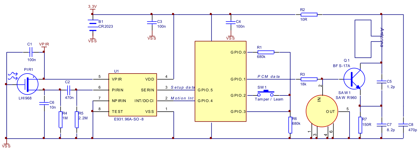
Fig 1: Wireless Intruder Detector
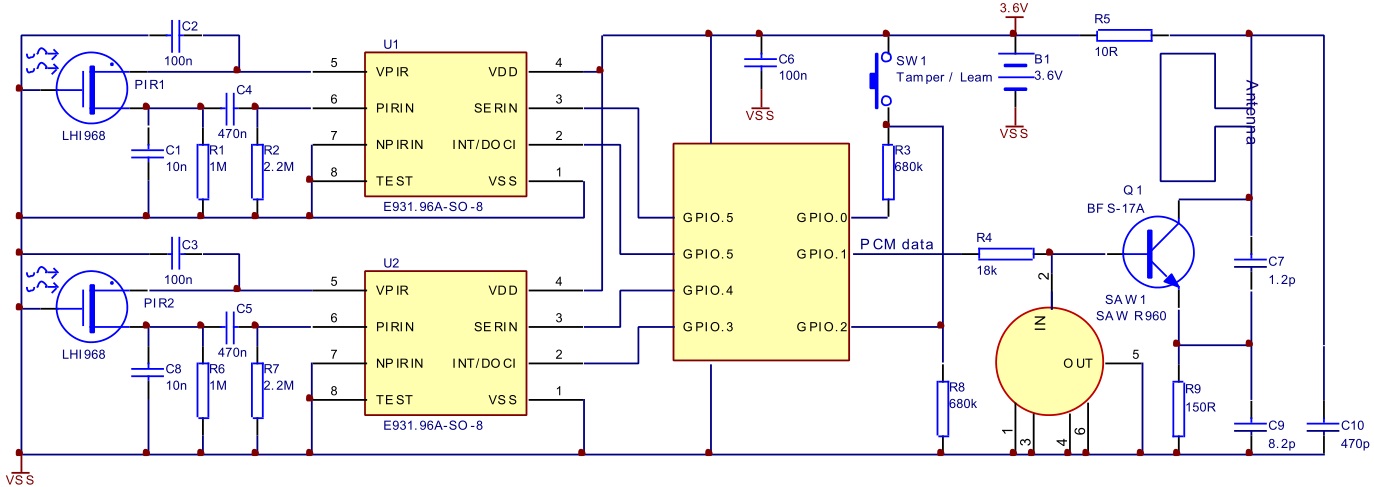
Fig 2:Wireless Intruder Detector with Two Controllers
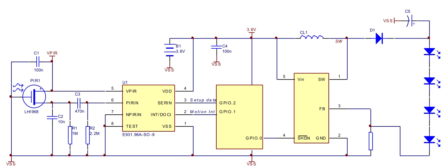
Fig 3: Emergency Lighting
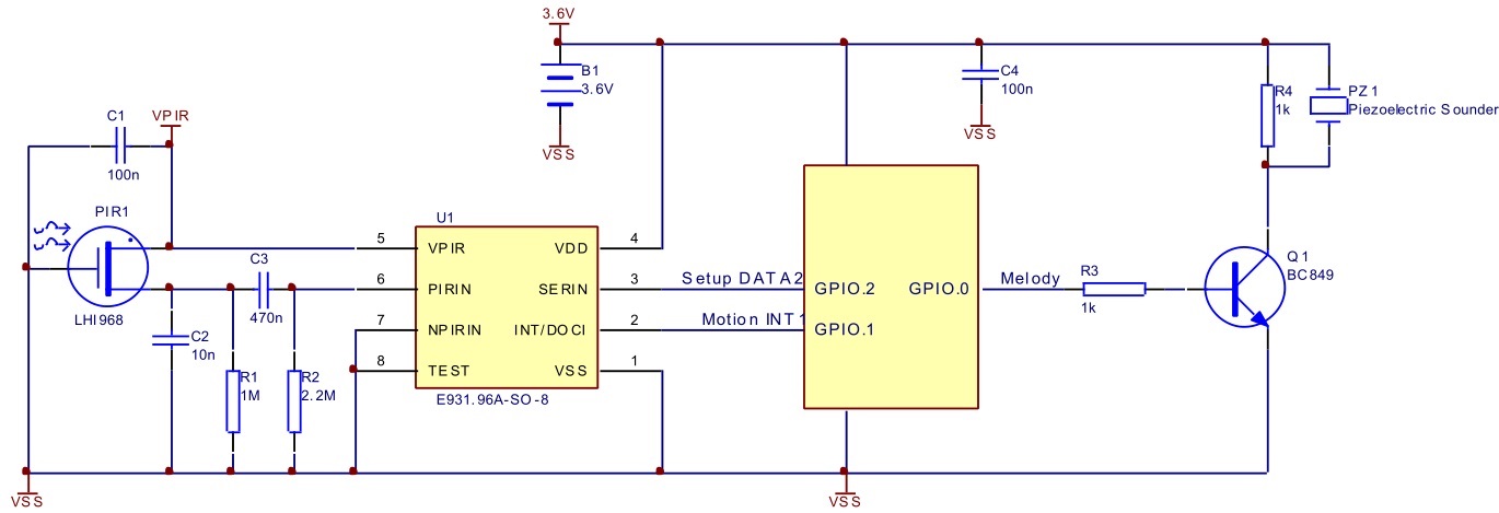
Fig 4: Door Chime
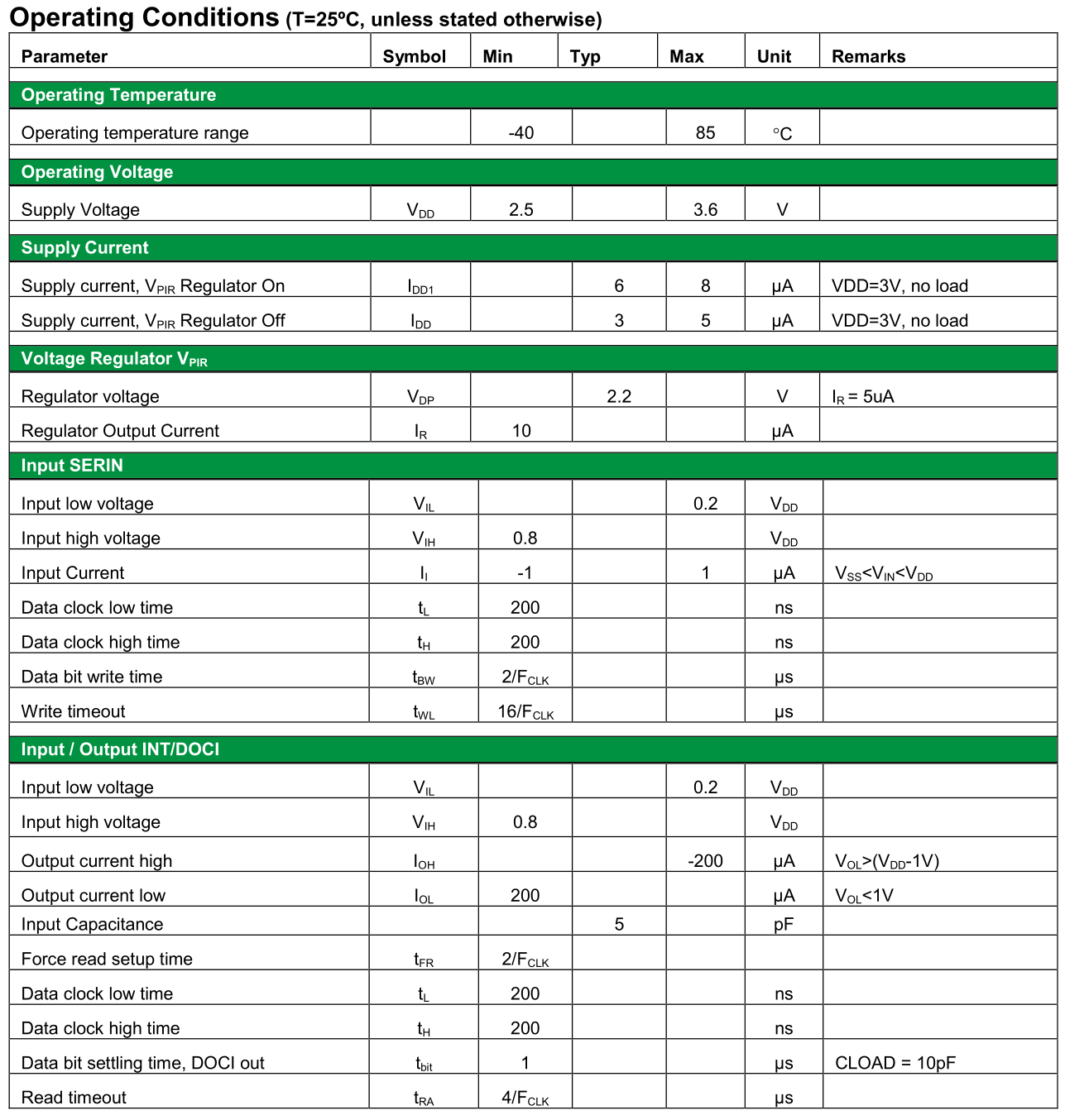
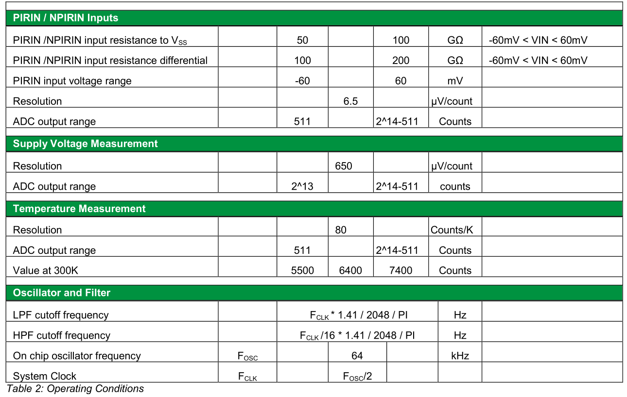
Electrical Characteristics
Detailed Description
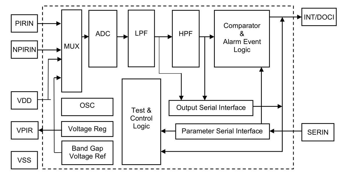
Fig 5: Block diagram of E931.96
MUX
The multiplexer selects the source signal for the ADC. It can select between the differential PIR inputs, differential temperature sensor output and asymmetrical supply voltage divider.
Voltage Regulator
The integrated voltage regulator provides a regulated 2.2V supply for an externally connected conventional PIR detector. The regulator can be activated through the control register.
Bandgap Voltage Reference
The bandgap voltage reference provides constant reference currents and voltages to the analog circuitry on chip across the specified operating temperature range of the device.
In addition, it contains a temperature voltage generator (temperature sensor).
Oscillator
The IC contains an on chip low power oscillator. The frequency is set to 64kHz. The timing signals and cutoff frequencies of the digital filters are derived from this frequency.
Band-Pass Filter
A 2nd order low-pass filter with a cut-off frequency of 7Hz eliminates unwanted higher frequency components. This signal is then passed to a 2 nd order high pass filter with a 0.4Hz cut-off frequency. Both filter output are accessible through the serial interface.
Alarm Event Logic
The signal from the band pass filter is rectified. When the signal level exceeds the sensitivity threshold, an internal pulse is generated. Subsequent pulses are counted, whenever the signals changes sign and exceeds the threshold again. The conditions for an alarm event such as the amount of pulses as well as the time window in which the pulses occur are programmable.
If an alarm event is cleared by resetting the interrupt output (by the device or through the external MCU), any motion detection is stopped during the programmable blind time. This feature is important to prevent self-triggering in applications, where high detection sensitivity is required.
Serial Interface
The device setup is done by programming setup registers via the SERIN pin. A simple clocked data-in protocol is used.Information from the device is read out with the INT/DOCI pin. A similar clocked data-out protocol is used.
Configuration Register
The device contains a configuration register. Write access is through the serial input. Read access is performed through the interrupt output.
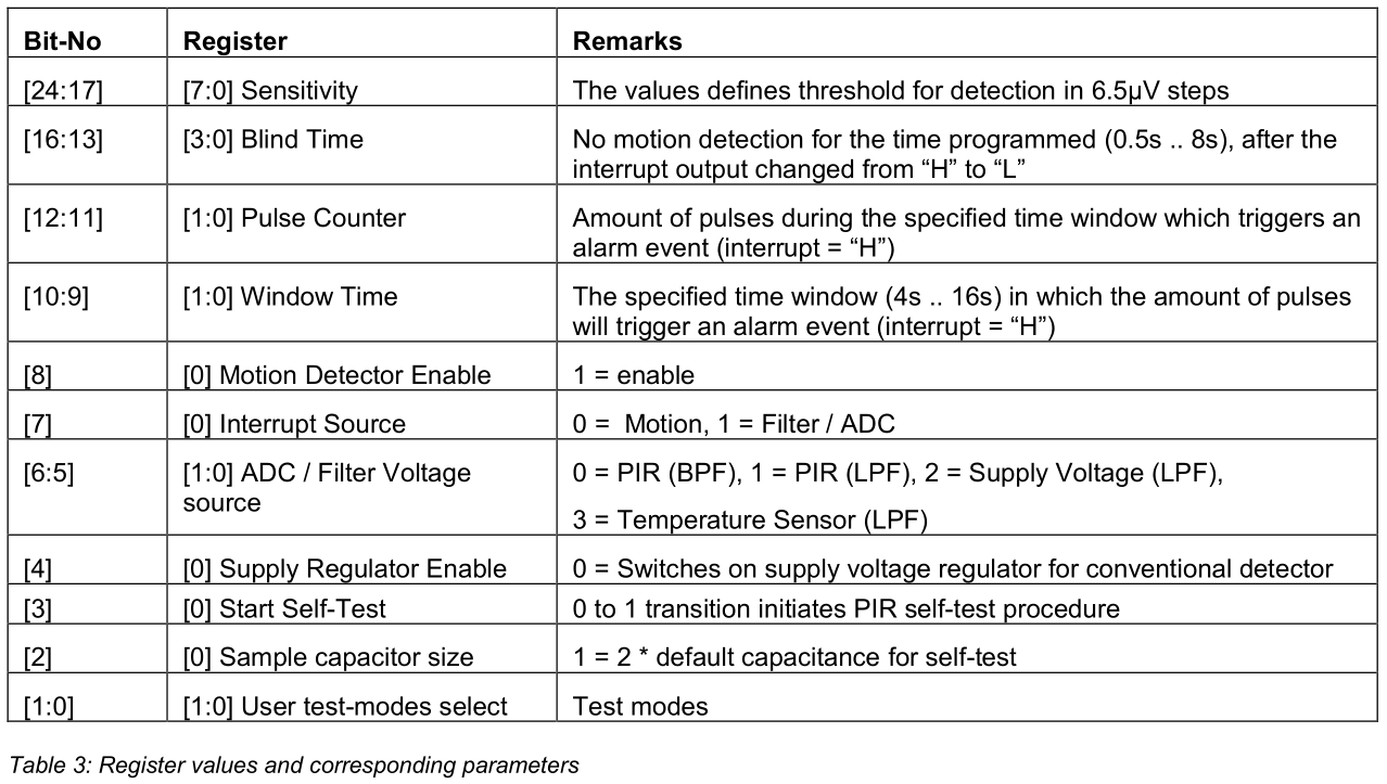
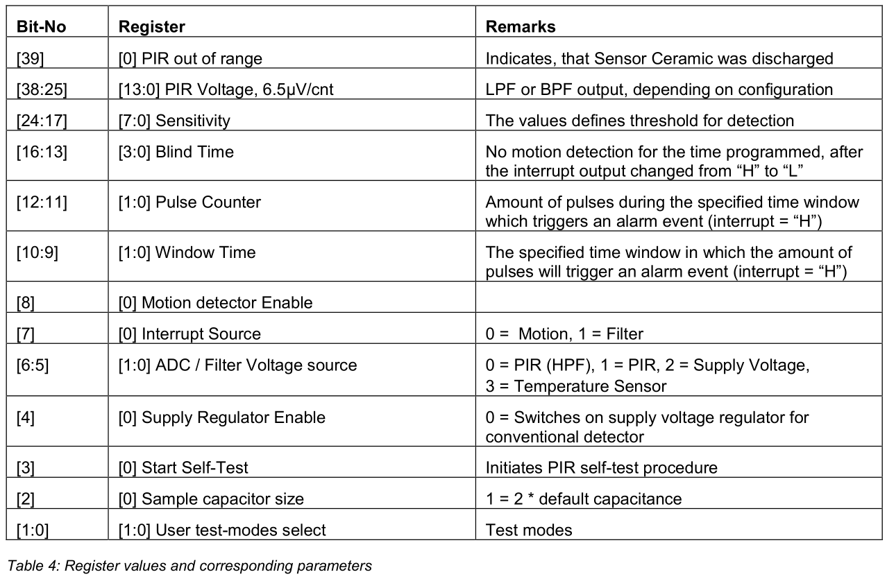
The following parameters can be adjusted through the control / configuration registers:
1. Sensitivity
The sensitivity / detection threshold is defined with the register value. The resolution of the register is 6.5µV.The threshold is [Register Value] * 6.5µV
2. Blind Time
Ignores motion after the interrupt output is switched back to 0
Range: 0.5s… 8s. The blind time is [Register Value] *0.5s
3. Programmable pulse counter
1… 4 pulses with sign change in between Amount of pulses = [Register Value] + 1
4. Window time
For noisy environments 4s… 16s window Window time = [Register Value] * 4s + 4s
5. Motion Detect Enable
0 = disable, 1 = enabled
6. Interrupt Source
The interrupt source can be selected between Motion (default) or ADC Decimation Filter. If the decimation filter is selected, interrupts are generated every 14ms. 0 = Motion, 1 = Filter
The Interrupt can be switched off by setting the mask bit to Motion and switching off the motion detector function.
7. Voltage Source
There is only one ADC integrated on chip. The following source voltages are selectable for the ADC:
PIR Signal, BFP Output = 0
PIR Signal, LPF Output = 1
Chip Supply Voltage = 2
On Chip Temperature Sensor = 3
For Motion Detector Mode, ‘0’ or ‘1’ has to be selected.
8. Supply Regulator Enable for conventional PIR Detector (2.2V)
Supply a regulated 2.2V on the V REG output.
1 = disabled, 0 = enabled
9. Start Self-Test
Initiates PIR self-test procedure that takes 2seconds to complete.
0 to 1 change = start
10. Sample Capacitor Value
For different size pyro ceramics, different sample capacitors can be selected for the pyro ceramic test
11. User test-modes
Reserved, program with 0
Serial Data Input
The configuration data is transferred into the device via the serial input. The external microcontroller has to generate a zero to one transition on the SERIN input and subsequently apply the data bit value (0/1). The ‘zero’ and ‘one’ time for the transition can be very short (1 instruction cycle of the microcontroller). The data bit value must be applied for at least 2 system clocks (t bit ) of the E931.96A. Whenever the transfer of data bits is interrupted for a period greater than 16 system clocks (t R ), the last data received is latched into the configuration register. The transmission of a 25 bit data should not be interrupted for more than 15 system clocks, as the device may latch the data already at this stage.
Fig 6: Serial Data clocked into device by MCU
Serial Data Output / Interrupt
The serial output serves as an Interrupt output, indicating motion and as a serial output for reading status and configuration data from the circuit.
Read Procedure
The E931.96 accepts readout with MCU defined timing. The MCU has to force DOCI to a high level for the duration of more than 2 device clock cycles (t FR ) and subsequently read out the data bits as described in the timing diagram below.Reading can be terminated at any time by forcing the DOCI line to “0” for at least 4 system clock cycles.
The interrupt source for the DOCI / INTR output can be selected between the ADC and the motions detect logic. If the ADC is selected, an interrupt is produced every 512 system clocks. If not, the alarm event logic will set the interrupt, whenever it detects motion AND motion detection is activated. No interrupt will be generated while the microcontroller accesses the interface.
Status and Configuration Data
The PIR voltage as well as all internal data can be read through the DOCI interface. The sequence of the data is fixed due to priority. The device outputs the PIR voltage value first, followed by status and configuration information. It is not required to read all data.
PIR Voltage Measurement
a) LPF Output
The ADC Source [6:5] has to be switched to the PIR inputs and the digital LPF output needs to be selected (=1).
V PIR = (ADC_out – ADC_offset) * 6.5µV.
b) HPF Output
The ADC Source [6:5] has to be switched to PIR input and the digital HPF output needs to be selected (=0).
V PIR = ADC_out * 6.5µV.
Supply Voltage Measurement
The ADC Source [6:5] has to be switched to Chip Supply (=2).
V DD = (ADC_out – ADC_offset) * 650µV.
Temperature Measurement
The ADC Source [6:5] has to be switched to the temperature sensor (=3).
Temperature = Tcal + (ADC_out – ADC_offset(Tcal)) / 80 * counts/K
ADC_offset = ADC value @ VIN = 0, typical value = 2^13
ADC_offset(Tcal) = ADC value at defined ambient temperature, typical value = 6400@300K

