Author Archives: Ameisina

About Ameisina

I am living shenzhen the 4th biggest city in china. I do some business with some friends and customers oversee. I try to intruduce the biggest E-component market in the world it's HUAQIANGBEI. I will express with seriess with the life here and the merchanter How they Living for. The most importance parts is I will intruduce the thousands components , parts and device.

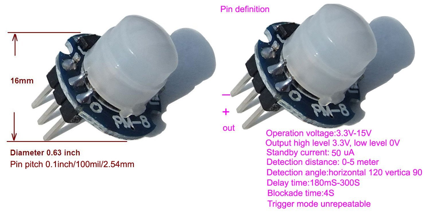
User Guide DWM-PM-8 50uA Lowest standby Current 0.18s to 300s Delay Time Mini Infrared PIR motion sensor module

DWM-PM-8 50uA Lowest standby Current 0.18s to 300s Delay Time Mini Infrared PIR motion sensor module

Features

Power supply is 3.3V to 15V.module include LDO;
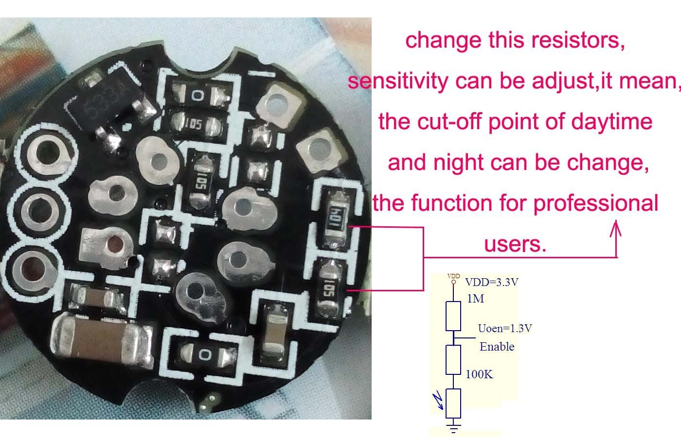
Sensitivity can be adjust,
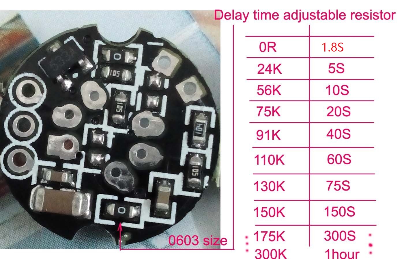
Delay time can be adjust,
Trigger mode is be defined as repeatable;
Controller MCU built-in sensor:strong interference rejection capacity,Low EMI.
[small size,Wideer working voltage range,small current,stable performance]

dwmzone-pir-infrared-sensor416-dwm-pm-8-50ua-lowest-standby-current-018s-to-300s-delay-time-mini-infrared-pir-motion-sensor-feature

dwmzone-pir-infrared-sensor416-dwm-pm-8-50ua-lowest-standby-current-018s-to-300s-delay-time-mini-infrared-pir-motion-sensor-feature

Repeatable: if the moudul detect human body is moving,output high level at once,this moment,at delay time,if PIR detect body is moving once more, then delay time reset,be cleared to zero,start counting from zero,until the delay time to over,will output low level,waitting next trigger.

Unrepeatle:if the moudul detect human body is moving,output high level at once,this moment,signal input line be closed,PIR detect is disabled, until the delay time to over,will output low level,waitting next trigger.

 LDR worke mode

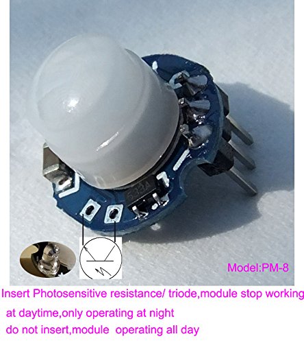
Customer can sold a LDR then the module will not work at the day time and will work at the evening.

dwmzone-pir-infrared-sensor416-dwm-pm-8-50ua-lowest-standby-current-018s-to-300s-delay-time-mini-infrared-pir-motion-sensor-module

dwmzone-pir-infrared-sensor416-dwm-pm-8-50ua-lowest-standby-current-018s-to-300s-delay-time-mini-infrared-pir-motion-sensor-moduleSensitivity adjust and Delay time adjust

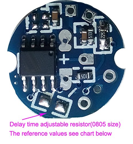
Sensitivity adjust and Delay time adjust

dwmzone-pir-infrared-sensor416-dwm-pm-8-50ua-lowest-standby-current-018s-to-300s-delay-time-mini-infrared-pir-motion-module

dwmzone-pir-infrared-sensor416-dwm-pm-8-50ua-lowest-standby-current-018s-to-300s-delay-time-mini-infrared-pir-motion-module

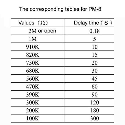
dwmzone-pir-infrared-sensor416-dwm-pm-8-50ua-lowest-standby-current-018s-to-300s-delay-time-mini-infrared-pir-motion-time-table

dwmzone-pir-infrared-sensor416-dwm-pm-8-50ua-lowest-standby-current-018s-to-300s-delay-time-mini-infrared-pir-motion-time-table

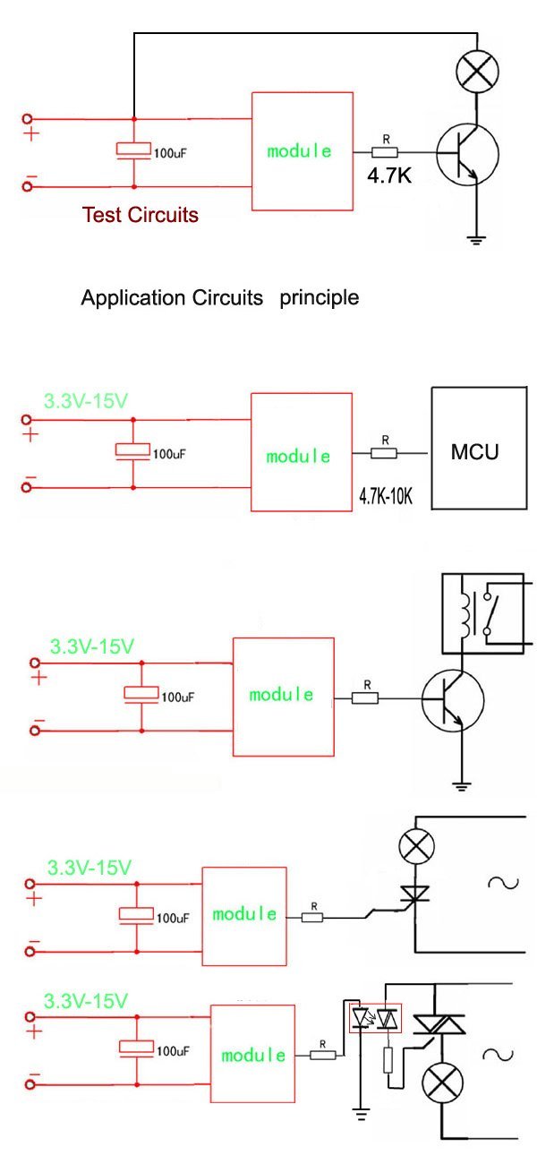
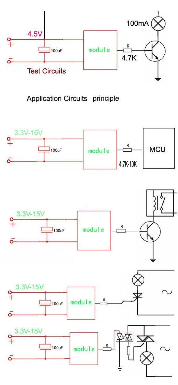
Test and Application circut

dwmzone-pir-infrared-sensor416-dwm-pm-8-50ua-lowest-standby-current-018s-to-300s-delay-time-mini-infrared-pir-motion-sensor-application

dwmzone-pir-infrared-sensor416-dwm-pm-8-50ua-lowest-standby-current-018s-to-300s-delay-time-mini-infrared-pir-motion-sensor-application

Motion Activated LED Step Light, Part 1 – Project Overview

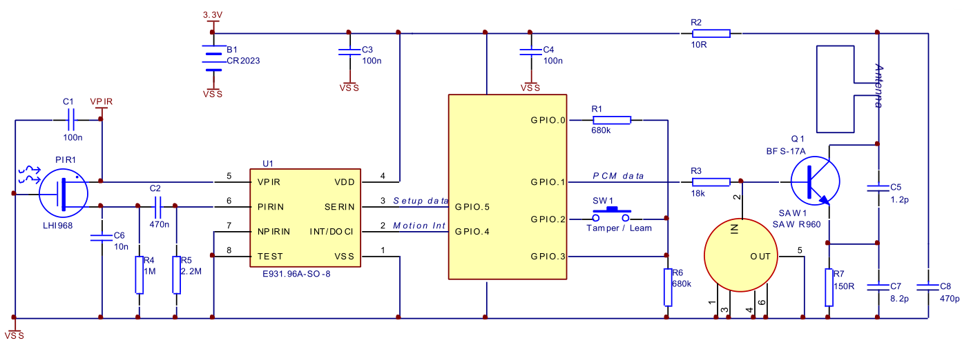
Motion Activated LED Step Light, Part 2 – PM-8 Sensor and Schematic

Motion Activated LED Step Light, Part 3 – Adding LIght Sensor (LDR)

Motion Activated LED Step Light, Part 4 – Warm white LEDs and battery life


Funding Support for Prototypes Service

Funding Support for Prototypes Service

Service

 Good ideas are just like a The fleeting meteors in the sky how can we catch it and make it comes to real world? Idea worth express.Funding Support for Prototypes Service target the electronic world.If you have a good idea just let us know we will help you to design and make it comes to truth only if we also think it’s good or you can approve it’s good,If you already have finished a design just let us know we can help you to make prototype for free only if we think it can get people educated or bring the benefit to people’s life or work.

Possibility

Our team set at the City Shenzhen,Guangdong,China where has the largest electronics market which name is HUAQIANGBEI  You can find anything electronic parts here within five minutes at a small counter which  spread over the market.Here it also has a full mature supply chain,we can gurantee that we can offer an professional,Experienced and fast service.

Implementation

We are going to fully use the social network media to get further exposure to our service. Funding Support for Prototypes Group at FacebookFunding Support for Prototypes at the communities of google+instructables project.We have online store which is Dwmzone whih will help to sell the prototypes.we have a Venture capital team who is going to funding for the prototypes,We have a experienced engineers team who is going to offer a profesional consultant service for the coming ideas and design.We also have  has a supply chain manager team who is going to gurantee a fast manufacture and delivery service.


Funding Support for Prototypes-facebook

Funding Support for Prototypes-facebook


Funding Support for Prototypes-google+

Funding Support for Prototypes-google+

 Funding-Support-for-Prototypes-instuctable-1.png March 8, 2017 230 KB 994 × 529 Edit Image Delete Permanently URL http://odlstore.com/blog/wp-content/uploads/2017/02/Funding-Support-for-Prototypes-instuctable-1.png Title Funding Support for Prototypes-instuctable Caption Funding Support for Prototypes-instuctable Alt Text

Funding Support for Prototypes-instuctable

Process

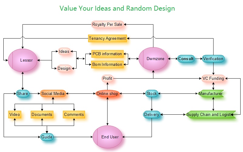
dwmzone-Value-your-ideas-and-random-design-Royalty

dwmzone-Value-your-ideas-and-random-design-Royalty

Let me explain the whole process simply.

Ownership

Lessors own the ideas and designs Dwmzone will rent the ideas or designs In a certain period of time(one or three years) after that the Dwmzone will release the ownership back to the Lessors.

Division of labour

Lessors

Turn the ideas and design into a Required PCB information and Required Bom information send to Dwmzone.Share the software to the End Users and Shoot a video give an introduction about the design and ideas and guide the End Users how to use it.reply the comments and answer the questions.

Dwmzone

Give lessors a professional consultancy make it more practicable and turn the ideas and design to a real products,Sign a Tenancy agreement with Lessors which will write down the lease period and  Percentage for paid royalty (we will pay you a percentage-based royalty per product sold), Offer a vc funding and charge the manufacture ,stock,delivery and sell around the word.

Endusers

Pay for the service, got the benefit and fun.

Idea worth express this is a great journey join with us start the big adventure

For further information please contact us:

DWMZONE LIMITED .

E-mail: sales@odlstore.com     Skype: ameisina

Twitter:Dwmzone     Facebook:Dwmzone

Website: http://www.odlstore.com


User Guide for DWM-PM-6 20uA Lowest standby Current 1.8s to 1Hour Delay Time Mini Infrared PIR module

DWM-PM-6 20uA Lowest standby Current 1.8s to 1Hour Delay Time Mini Infrared PIR module

Features

Power supply is 3.3V to 15V.module include LDO;
Sensitivity can be adjust,
Delay time can be adjust,
Trigger mode is be defined as repeatable;
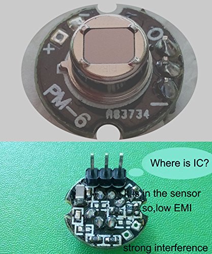
Controller MCU built-in sensor:strong interference rejection capacity,Low EMI.
[small size,Wideer working voltage range,small current,stable performance]

dwmzone-dwm-pm-6-20ua-lowest-standby-current-18s-to-1hour-delay-time-mini-infrared-pir-module-delay-time-low-EMI

dwmzone-dwm-pm-6-20ua-lowest-standby-current-18s-to-1hour-delay-time-mini-infrared-pir-module-delay-time-low-EMI

Repeatable: if the moudul detect human body is moving,output high level at once,this moment,at delay time,if PIR detect body is moving once more, then delay time reset,be cleared to zero,start counting from zero,until the delay time to over,will output low level,waitting next trigger.

Unrepeatle:if the moudul detect human body is moving,output high level at once,this moment,signal input line be closed,PIR detect is disabled, until the delay time to over,will output low level,waitting next trigger.

 LDR worke mode

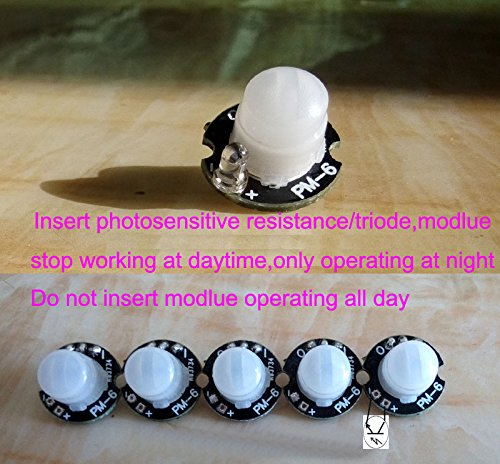
Customer can sold a LDR then the module will not work at the day time and will work at the evening.

dwmzone-dwm-pm-6-20ua-lowest-standby-current-18s-to-1hour-delay-time-mini-infrared-pir-module

dwmzone-dwm-pm-6-20ua-lowest-standby-current-18s-to-1hour-delay-time-mini-infrared-pir-module

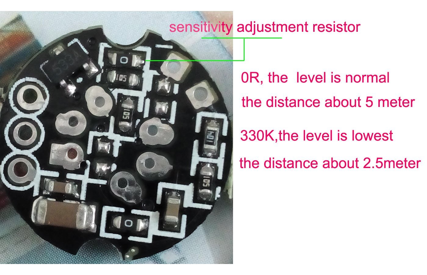
Sensitivity adjust and Delay time adjust

dwmzone-dwm-pm-6-20ua-lowest-standby-current-18s-to-1hour-delay-time-mini-infrared-pir-module-sensitive

dwmzone-dwm-pm-6-20ua-lowest-standby-current-18s-to-1hour-delay-time-mini-infrared-pir-module-sensitive

dwmzone-dwm-pm-6-20ua-lowest-standby-current-18s-to-1hour-delay-time-mini-infrared-pir-module-delay-time

dwmzone-dwm-pm-6-20ua-lowest-standby-current-18s-to-1hour-delay-time-mini-infrared-pir-module-delay-time

dwmzone-dwm-pm-6-20ua-lowest-standby-current-18s-to-1hour-delay-time-mini-infrared-pir-module-delay-time-low-delay-time-1.8S

dwmzone-dwm-pm-6-20ua-lowest-standby-current-18s-to-1hour-delay-time-mini-infrared-pir-module-delay-time-low-delay-time-1.8S

Test and Application

dwmzone-dwm-pm-6-20ua-lowest-standby-current-18s-to-1hour-delay-time-mini-infrared-pir-module-application

dwmzone-dwm-pm-6-20ua-lowest-standby-current-18s-to-1hour-delay-time-mini-infrared-pir-module-application

Note:

1.Before use,need checking Solder iron temperature , implement leakage of electricity, and static discharge in winter(cmos component)
2.When power on,IC has 20S to 60S self-testing process,in the meantime,will output high level,then,output low level,into stable waiting state.(waiting state,it is also on standby);

3.The module ouput is MCU IO port direct output,to use,advise series connection a resistance,4.7K to 10K;

Software development guide for E931.96, Reading and Writing functions

Affected Devices and Sensors

E931.96 Ultra-Low Power PIR Controller

Interfaces

The E931.96 accepts data from the MCU on the SERIN input pin. Measurement data is clocked out and motion interrupts are flagged on the INT/DOCI pin of the device.A zero to one transition on the INT output indicates detected motion. The interrupt pin will stay at one until it is cleared by the MCU.The MCU can read the ADC voltages (14 bits) and the configuration data (25bits) through the DOCI output of the E931.96.

Setting up the device (SERIN)

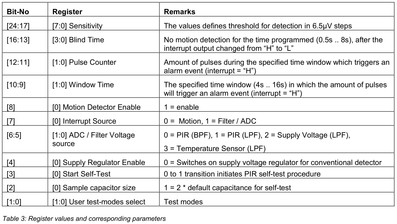
After power up the E931.96 need to be programmed with a configuration that sets up the device with operational parameters and puts the device in the correct operational mode.  The device is programmed with a 25-bit bit stream on the SERIN input. The SERIN input is held low when the interface is not used, it also provides for minimum interference to the sensor. The microcontroller generates a low to high transition on the SERIN input, this is a clock pulse, and subsequently applies a data bit value, either a one or a zero. This process is repeated 25 times until all the data bits are clocked into the E931.96. The low to high transition or clock pulse can be very short, typically 1 instruction cycle of the microcontroller, but the data bit value must be applied for at least 2 system clocks (2/FCLK), of the E931.96. Whenever the data transfer is interrupted for more than 16 system clocks (16/FCLK), the last data received is latched into the configuration registers. Should the transfer of data be interrupted for more than 15 system clocks, the writing procedure needs to be restarted.Table 3 in the datasheet shows the sequence of bits and the meaning of the register values. Configuration data is clocked into the device starting at bit 24 down to bit 0.  A typical code example would look as follows:

void write_to_E93196(long long setup_data)  // setup_data holds the device configuration

{

char i;

long long mask;

mask=0x01000000;       // Bitmask is at bit 25

for(i=0;i<25;i++)

{

serin_clock();        // Generates zero to one clock pulse on SERIN pin

if((setup_data&mask)>0)  // Decide if it is a one or a zero data bit

output_high(SERIN);

else

output_low(SERIN);

delay_us(72);         // More than 62us, ensure it is more than 2/FCLK

mask>>=1;            // Shift mask to the next bit

}

output_low(SERIN);

delay_ms(1);            // Wait for data to be latched, time must be more than 16/FCLK

}

Reading

The DOCI pin is used to transfer data from the device to the MCU. The MCU drives a clock signal and the E931.96 provides the data bit. The MCU initiates reading of the status and configuration data by forcing a high level for the duration of more than 2 device clock cycles (>3/FCLK) on the DOCI pin (tFR in the datasheet).

A clock pulse is generated by a low to high transition on the DOCI pin. Subsequently the MCU samples data bit value driven by the E931.96. This process is repeated 15 times to read the ADC value and a further 25 times until all the data bits are clocked out of the E931.96. The sampling speed is influenced by the capacitance on the DOCI line due to the PCB layout and the MCU load. The DOIC pin does not have a strong driver so that it can be overdriven for the clock pulses. When readout is completed, the MCU must drive the DOCI pin to zero, and subsequently switch to tri-state in order to receive a new interrupt. The source for the ADC input can be selected between PIR input, supply voltage input and temperature. Reading can be terminated at any time by forcing the DOCI line to zero for at least 4 system clock cycles.The interrupt source for the DOCI/INT output can be selected between reading of the ADC values or for motion detection. If the ADC interrupt is selected, an interrupt is produced every 512 system clocks that signals that an ADC value is available to be clocked out. It is possible to read ADC values without making use of the interrupts generated by the E931.96.For interrupts as a result of motion, the motion detection bit and the interrupt source bit need to be set.No interrupt will be generated while the microcontroller accesses the interface.Below is an example of reading the ADC value as well as the configuration data from the device.

void readback_all_from_E93196(void)

{

int n;

long long kk;

#use fast_io(A)  // This tells the compiler that I will take care of the direction settings of the port

force_doci_high();   // force read, hold DOCI high at least 3 clocks of IC

//clock out bits [39:25] for the ADC value and the out of range bit

for(n=0;n<(14+1);n++)

{

doci_clock();

adc<<=1;     // This instruction is my sample delay

if(input(DOCI_PIN)==1)

adc++;

}

//Next read the setup bits [24:0]

setup_back=0;

for(n=0;n<25;n++)

{

doci_clock();

kk<<=1;          // This instruction is my sample delay

if(input(DOCI_PIN)==1)

setup_back++;

}  clear_DOCI_interrupt();

#use standard_io(A)

}

Helper functions

In the examples above we made use of small functions that is shown below. The syntax of these functions may be different to suit the particular compiler that is used. The DOCI output is clocked by the device as fast as possible; the direction handling is also taken care of.

void doci_clock(void)

{

#use fast_io(A)

output_low(DOCI_PIN);     // Clear DOCI pin

doci_dir&=~DOCI_PIN_DIR;  // Clear direction bit

set_tris_a(doci_dir);     // DOCI pin output

delay_cycles(5);          // Wait a bit

output_high(DOCI_PIN);    // Set DOCI pin

doci_dir|=DOCI_PIN_DIR;   // Set direction bit

set_tris_a(doci_dir);     // DOCI pin input

delay_cycles(5);          // Wait a bit

}

After an interrupt was generated by the device, it is cleared by the MCU by driving the DOIC pin low and releasing it, so that the device can drive again when an interrupt occurs.

void clear_DOCI_interrupt(void)

{

//Release the DOCI Line leave in zero state

#use fast_io(A)    // Prevent compiler from handling the direction control

output_low(DOCI_PIN);      // Clear DOCI pin

doci_dir&=~DOCI_PIN_DIR;   // Clear direction bit

set_tris_a(doci_dir);      // DOCI pin output

delay_cycles(175);      // Time depends on track capacitance on the PCB

doci_dir|=DOCI_PIN_DIR;    // Set direction bit

set_tris_a(doci_dir);      // DOCI pin input

#use standard_io(A)

}

A read request from the MCU to the E931.96 is indicated by forcing DOCI to high level for 3 device clocks (3/FCLK) of the E931.96

void force_doci_high(void)

{

// force read, at least 3 clocks of IC

#use fast_io(A)    // Prevent compiler from handling the direction control

output_high(DOCI_PIN);    // Set DOCI pin

doci_dir&=~DOCI_PIN_DIR;  // Clear direction bit

set_tris_a(doci_dir);     // DOCI pin output

delay_us(120);

#use standard_io(A)

}

The function below generates the clock signal on the SERIN input of the device. The clock delay can be as short as one cycle on the MCU.

void serin_clock(void)

{

output_low(SERIN); // Clear SERIN pin

delay_us(1);

output_high(SERIN);     // Set SERIN pin

delay_us(1);

}
E931.96 Ultra-Low Power PIR Controller Integrated Circuit

E931.96 Ultra-Low Power PIR Controller

General Description

The E931.96 is an ultra-low power motion detector controller integrated circuit. The device is ideally suited for battery operated wireless motion sensors that make use of an MCU for handling communication. The MCU does not need to be active while the E931.96 does continuous motion sensing. It only activates the external controller, when motion is
detected. Motion is signaled through the push-pull output (INT). The criteria for motion detection are programmable and can be changed by the external controller.
The E931.96 interfaces directly with up to two conventional PIR sensors via a high impedance
differential input. The PIR signal is converted to a 14 bit digital value on chip.All signal processing is performed digitally.The E931.96 is available in a SOIC-8 package.

Applications

 Wireless intruder detectors
 Battery powered door chimes
 Emergency lighting
 Motion and presence detection

Features

 Programmable detection criteria and operating modes
 Digital signal processing
 On chip supply regulator for conventional PIR detectors
 Ultra Low power consumption
 Differential PIR sensor input
 Supply voltage measurement
 Temperature measurement
 Instantaneous settling after power up

Application Circuits

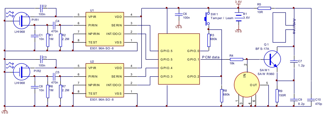
dwmzone-e931.96-Application-Circuits-1

Fig 1: Wireless Intruder Detector

Fig 1: Wireless Intruder Detector

Wireless Intruder Detector with Two Controllers

Fig 2:Wireless Intruder Detector with Two Controllers

Fig 2:Wireless Intruder Detector with Two Controllers

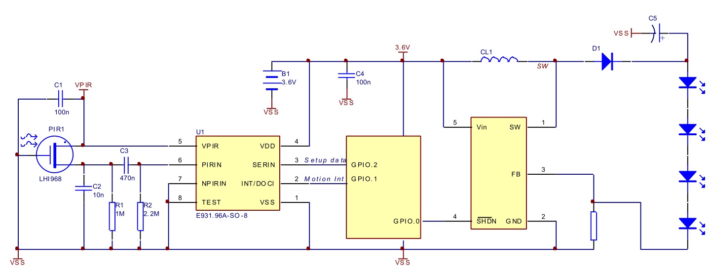
Emergency Lighting

Emergency Lighting

Fig 3: Emergency Lighting

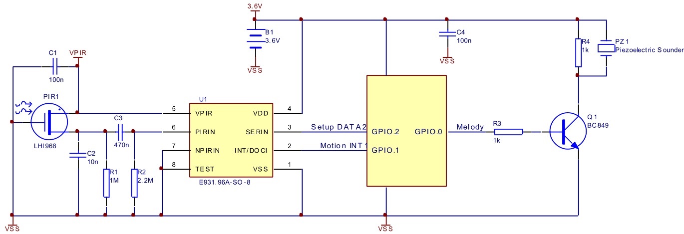
Door Chime

Door ChimeFig 4: Door Chime

Fig 4: Door Chime


Electrical Characteristics

Absolute Maximum Ratings

Absolute Maximum Ratings

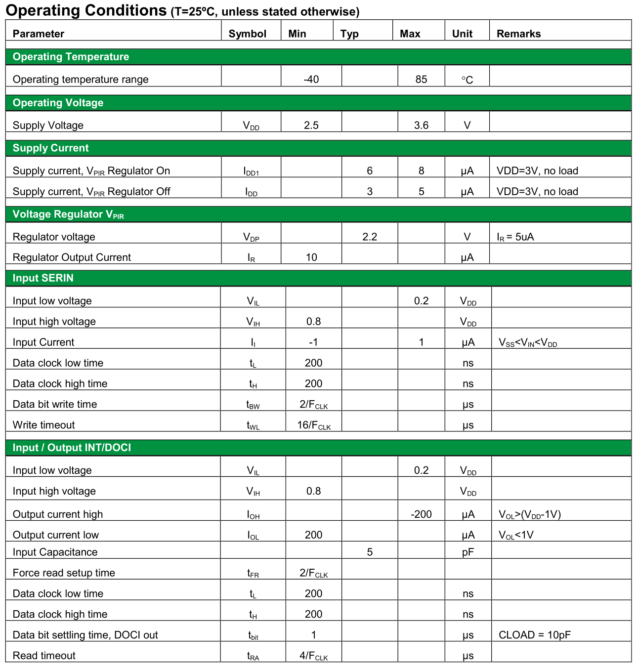
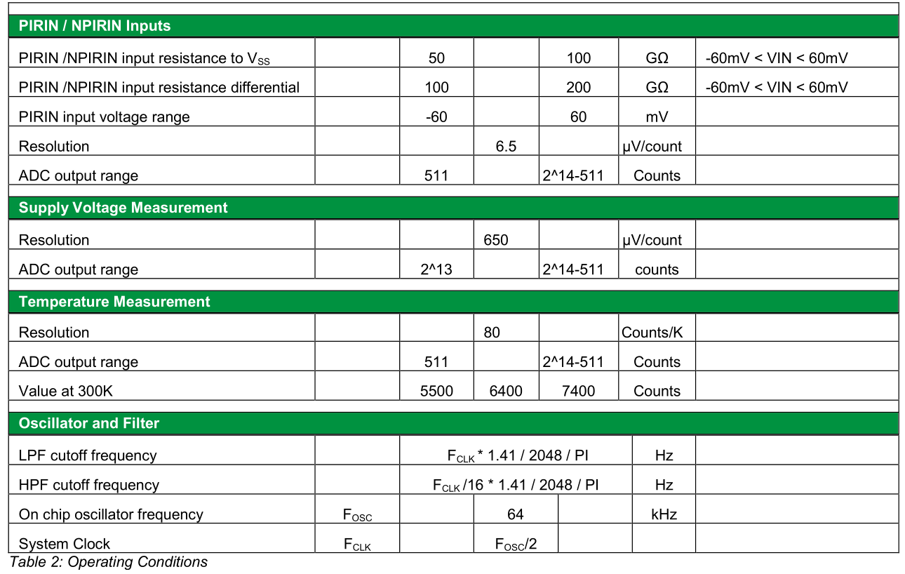
Operating Conditions

Operating Conditions

Operating Conditions

Operating Conditions

Detailed Description

Detailed Description

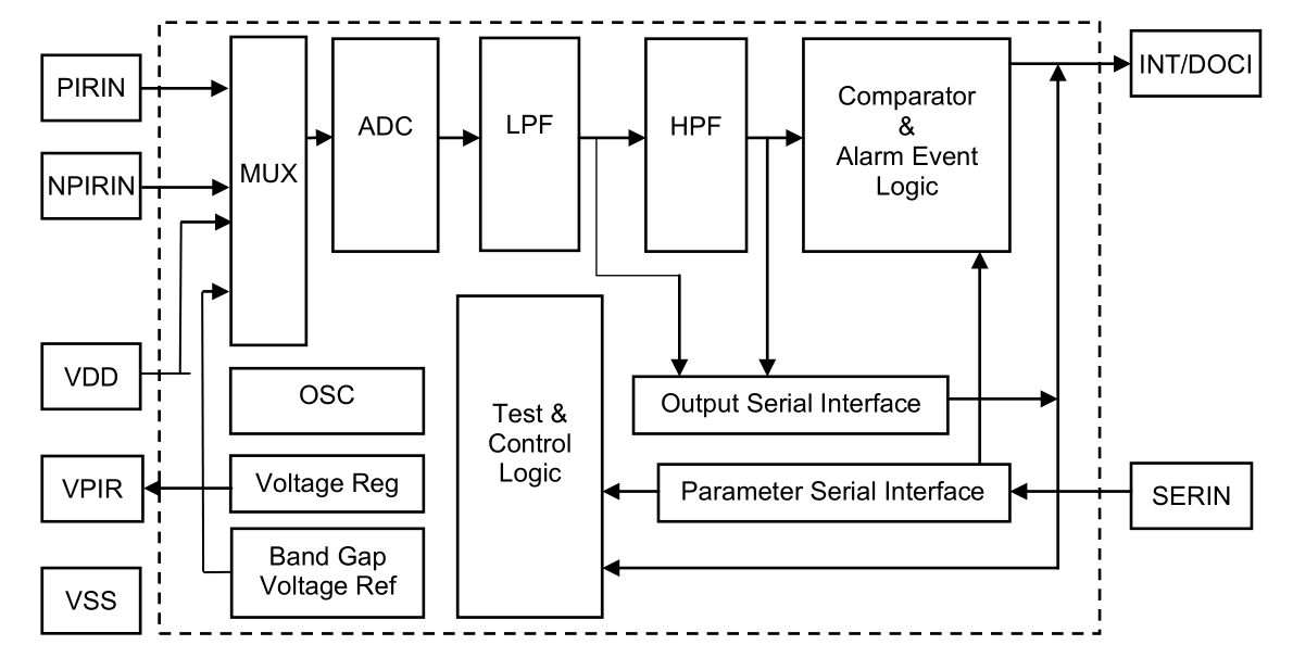
Fig 5: Block diagram of E931.96

Fig 5: Block diagram of E931.96

MUX

The multiplexer selects the source signal for the ADC. It can select between the differential PIR inputs, differential temperature sensor output and asymmetrical supply voltage divider.

Voltage Regulator

The integrated voltage regulator provides a regulated 2.2V supply for an externally connected conventional PIR detector. The regulator can be activated through the control register.

Bandgap Voltage Reference

The bandgap voltage reference provides constant reference currents and voltages to the analog circuitry on chip across the specified operating temperature range of the device.
In addition, it contains a temperature voltage generator (temperature sensor).

Oscillator

The IC contains an on chip low power oscillator. The frequency is set to 64kHz. The timing signals and cutoff frequencies of the digital filters are derived from this frequency.

Band-Pass Filter

A 2nd order low-pass filter with a cut-off frequency of 7Hz eliminates unwanted higher frequency components. This signal is then passed to a 2 nd order high pass filter with a 0.4Hz cut-off frequency. Both filter output are accessible through the serial interface.

Alarm Event Logic

The signal from the band pass filter is rectified. When the signal level exceeds the sensitivity threshold, an internal pulse is generated. Subsequent pulses are counted, whenever the signals changes sign and exceeds the threshold again. The conditions for an alarm event such as the amount of pulses as well as the time window in which the pulses occur are programmable.
If an alarm event is cleared by resetting the interrupt output (by the device or through the external MCU), any motion detection is stopped during the programmable blind time. This feature is important to prevent self-triggering in applications, where high detection sensitivity is required.

Serial Interface

The device setup is done by programming setup registers via the SERIN pin. A simple clocked data-in protocol is used.Information from the device is read out with the INT/DOCI pin. A similar clocked data-out protocol is used.

Configuration Register

The device contains a configuration register. Write access is through the serial input. Read access is performed through the interrupt output.
The following parameters can be adjusted through the control / configuration registers:

1. Sensitivity

The sensitivity / detection threshold is defined with the register value. The resolution of the register is 6.5µV.The threshold is [Register Value] * 6.5µV

2. Blind Time

Ignores motion after the interrupt output is switched back to 0
Range: 0.5s… 8s. The blind time is [Register Value] *0.5s

3. Programmable pulse counter

1… 4 pulses with sign change in between Amount of pulses = [Register Value] + 1

4. Window time

For noisy environments 4s… 16s window Window time = [Register Value] * 4s + 4s

5. Motion Detect Enable

0 = disable, 1 = enabled

6. Interrupt Source

The interrupt source can be selected between Motion (default) or ADC Decimation Filter. If the decimation filter is selected, interrupts are generated every 14ms. 0 = Motion, 1 = Filter
The Interrupt can be switched off by setting the mask bit to Motion and switching off the motion detector function.

7. Voltage Source

There is only one ADC integrated on chip. The following source voltages are selectable for the ADC:
PIR Signal, BFP Output = 0
PIR Signal, LPF Output = 1
Chip Supply Voltage = 2
On Chip Temperature Sensor = 3
For Motion Detector Mode, ‘0’ or ‘1’ has to be selected.

8. Supply Regulator Enable for conventional PIR Detector (2.2V)

Supply a regulated 2.2V on the V REG output.
1 = disabled, 0 = enabled

9. Start Self-Test

Initiates PIR self-test procedure that takes 2seconds to complete.
0 to 1 change = start

10. Sample Capacitor Value

For different size pyro ceramics, different sample capacitors can be selected for the pyro ceramic test

11. User test-modes

Reserved, program with 0

Serial Data Input

The configuration data is transferred into the device via the serial input. The external microcontroller has to generate a zero to one transition on the SERIN input and subsequently apply the data bit value (0/1). The ‘zero’ and ‘one’ time for the transition can be very short (1 instruction cycle of the microcontroller). The data bit value must be applied for at least 2 system clocks (t bit ) of the E931.96A. Whenever the transfer of data bits is interrupted for a period greater than 16 system clocks (t R ), the last data received is latched into the configuration register. The transmission of a 25 bit data should not be interrupted for more than 15 system clocks, as the device may latch the data already at this stage.

Serial Data clocked into device by MCU

Serial Data clocked into device by MCU

Fig 6: Serial Data clocked into device by MCU

Register values and corresponding parameters

Register values and corresponding parameters

Serial Data Output / Interrupt

The serial output serves as an Interrupt output, indicating motion and as a serial output for reading status and configuration data from the circuit.

Read Procedure

The E931.96 accepts readout with MCU defined timing. The MCU has to force DOCI to a high level for the duration of more than 2 device clock cycles (t FR ) and subsequently read out the data bits as described in the timing diagram below.Reading can be terminated at any time by forcing the DOCI line to “0” for at least 4 system clock cycles.

Timing diagram for the DOCI interface

Timing diagram for the DOCI interface

The interrupt source for the DOCI / INTR output can be selected between the ADC and the motions detect logic. If the ADC is selected, an interrupt is produced every 512 system clocks. If not, the alarm event logic will set the interrupt, whenever it detects motion AND motion detection is activated. No interrupt will be generated while the microcontroller accesses the interface.

Status and Configuration Data

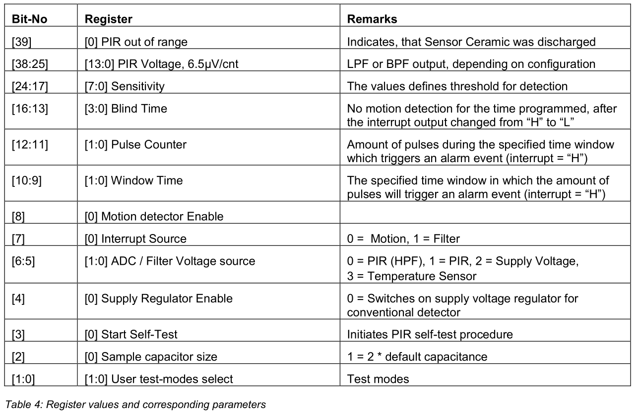
The PIR voltage as well as all internal data can be read through the DOCI interface. The sequence of the data is fixed due to priority. The device outputs the PIR voltage value first, followed by status and configuration information. It is not required to read all data.

Data words available on DOCI interface

Data words available on DOCI interface

Register values and corresponding parameters

Register values and corresponding parameters

PIR Voltage Measurement

a) LPF Output
The ADC Source [6:5] has to be switched to the PIR inputs and the digital LPF output needs to be selected (=1).
V PIR = (ADC_out – ADC_offset) * 6.5µV.
b) HPF Output
The ADC Source [6:5] has to be switched to PIR input and the digital HPF output needs to be selected (=0).
V PIR = ADC_out * 6.5µV.

Supply Voltage Measurement

The ADC Source [6:5] has to be switched to Chip Supply (=2).
V DD = (ADC_out – ADC_offset) * 650µV.

Temperature Measurement

The ADC Source [6:5] has to be switched to the temperature sensor (=3).
Temperature = Tcal + (ADC_out – ADC_offset(Tcal)) / 80 * counts/K
ADC_offset = ADC value @ VIN = 0, typical value = 2^13
ADC_offset(Tcal) = ADC value at defined ambient temperature, typical value = 6400@300K

SOIC8 Pin Out

SOIC8 Pin Out

SOIC8 Pin Out